
New York City’s Times Square is known as the “Crossroads of the World.” Approximately 1.5 million people pass through the intersection of Broadway and 42nd Street every day, and millions more see the area daily on television broadcasts. No better place for outdoor advertising exists. As a result, dazzling signs have become a Times Square trademark.
Every advertiser wants to have the best advertising medium possible, so new signs must use the latest technology. Times Square tenants rely on MultiMedia, which manufactures the majority of the spectacular signs in Times Square. When MultiMedia asked our company, Advanced Electronic Designs, Inc. (AED), to design an LED sign for JPMorgan Chase™ in Times Square, we needed a huge amount of signal processing, data distribution, and interfacing. We also needed to design the sign very quickly. We met this challenge by utilizing the advantages of Xilinx® components.
We used Virtex-II™ XC2V1000 FPGAs for video processing, and for control and distribution we chose low-cost Spartan-3™ XC3S200 FPGAs. To configure the FPGAs, we chose the Platform Flash XCF00 configuration PROM family. And for final distribution of the data on the 3800 LED blocks, we used XC9572XL PLDs.
The Design
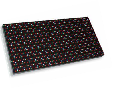
An LED sign is like a large computer monitor; video data goes in and is displayed on the sign. The sign comprises red, green, and blue LEDs that turn on and off (pulsewidth modulation) to generate more than four trillion colors.
What made this particular design a challenge was the scale, both in terms of physical size as well as the amount of data and the transfer rates involved. The sign is 135 feet long and 26 feet tall. With nearly two million pixels, it is the highest definition LED display in the world. This is ten times the resolution of the average television screen and twice the resolution of topof-the-line HDTV sets.
After considering our options, designing with Xilinx programmable logic was the obvious choice. The high-performance, low-cost FPGAs are well suited for all three main components of this design: video processing, data distribution, and sign control.
Video Processing
The video processor accepts a variety of video inputs. It captures these video streams as 36 bit RGB (12 bits per color). It then crops and places these inputs onto a master sign image for display. Color-space conversion adjusts image characteristics such as color temperature and balance. Additional processing corrects for individual LED differences. We also use proprietary image processing algorithms to operate the LEDs efficiently while maintaining optimal image quality.
Data Distribution
Video data starts in a control room and ends at the LEDs. The first step is the video processor, which is located in the control room. The video processor breaks the images into manageable chunks to send to the many modules of the sign so that each LED displays the data for the corresponding pixel. More than 3 Gbps of video data alone is required to operate the LEDs. In addition to video data, we also transfer a variety of control and status functions.
Not wanting to reinvent the wheel, we chose Ethernet as our data distribution medium. Our video processor has multiple Gigabit Ethernet ports that interface to the sign. Gigabit Ethernet can be transferred over fiber-optic cable, allowing great distances between the controller and the sign itself.
We were able to use off-the-shelf switches to distribute the data within the sign and put inexpensive 10/100 Ethernet ports on the individual distribution boards. The availability of Ethernet protocol analyzers, such as the open-source project Ethereal, allowed us to easily analyze and debug the system.
Sign control
In advertising, time is money; thus it is crucial to monitor the sign at all times. The control system monitors temperatures throughout the sign to ensure that adequate cooling is present. Voltages are monitored to detect malfunctioning power supplies. The control system maintains error and resend counts to detect faulty data links. It also provides an interface to upgrade the FPGAs remotely for enhancements and bug fixes.
The reconfigurable nature of Xilinx FPGAs allows us to provide feature upgrades and bug fixes to the customer via email…
The Benefits of Xilinx Devices
Xilinx devices include a large number of features that are ideal for our sign project:
- The reconfigurable nature of Xilinx devices is necessary for a project like this. Without FPGAs, the only alternative would have been an ASIC. But an ASIC was not feasible for this project for several reasons.
First, this project had a very tight schedule. An ASIC could not have been completed in the time allotted. Second, the volumes of the components in this sign are not of sufficient volume to hide the NREs of an ASIC. Third, an ASIC lacks the development opportunities of an FPGA. To me, as an engineer, this reason is the most important. No matter how much simulation you perform, there can always be unexpected bugs. In an ASIC, these bugs are expensive; in an FPGA, they can be fixed easily.
Another FPGA advantage is that it can meet future needs through feature upgrades; an ASIC cannot. The reconfigurable nature of Xilinx FPGAs allows us to provide feature upgrades and bug fixes to the customer via email, making it easy for them to apply to the sign. Through an Ethernet interface, the FPGA reprograms the Platform Flash configuration PROM and automatically reboots. - Video processing requires a large number of multiply operations. The video processor must perform color-space conversion and apply calibration coefficients in real time. It would require a large portion of FPGA logic resources to build multipliers. Instead, this can be done very efficiently by utilizing the embedded multipliers. Building pipelined processing structures with the embedded multipliers allowed us to easily meet the processing requirements.
- This design required a large variety of signaling standards. The flexible Xilinx I/O blocks allowed us to connect directly to a large number of different interfaces. Voltages ranged from standard 3.3V CMOS down to 1.5V HSTL. We required single-ended and differential interfaces. In some cases we could have used external driver and receiver parts, but that would have added complexity and cost to the product.
Other high-speed I/O interfaces, such as to the DDR 333 memory, would not have been possible without direct FPGA support. The digitally controlled impedance (DCI) modes were necessary on the high-speed single-ended traces. - With the high data rates involved and the many data interfaces, we had a large number of clock domains. The quantity of global clock nets available and the ability of the digital clock managers (DCMs) to synthesize clock frequencies made this easy. We also used the phase shift ability of the DCM to adjust sample times on various interfaces.
- Block RAM is my favorite resource in an FPGA. Without block RAM, there are two memory options. The first option is the logic slices, using flip-flops or distributed RAM, but this is expensive and slow for anything more than 16- to 32-bit addresses. The second option is external memory, such as SDRAM. SDRAM storage is generally in the range of tens to hundreds of megabytes, leaving a huge size gap between these two memory options.
Block RAM bridges this size gap. It can be used for a limitless number of things, from FIFOs for processing engines to loadable tables for data conversions. The flexible port-widths of block RAM allow you to use them individually or in efficient combinations. The dual-port capability makes them easy to use for transferring data between clock domains or sharing data. - While very powerful and convenient, the PLDs and Spartan-3 FPGAs are also very inexpensive. When combined with the development advantages, the low device price makes Xilinx devices unbeatable when developing high-performance embedded systems.
PicoBlaze Processors
Device hardware capabilities are essential for any design, but development tools and tricks are also very important. The favorite toy in our Xilinx bag-of-tricks is the PicoBlaze™ processor. We could not have completed the project in the time allowed without extensive use of the PicoBlaze processor. The sign contains an impressive count of more than 1,000 of these embedded processors, with nine different designs.
| 10 | XC2V1000 Virtex-II FPGA |
| 323 | XC3S200 Spartan-3 FPGA |
| 333 | XCF00 Platform Flash PROM |
| 3,800 | XC9572XL 72 macrocell PLD |
Table 1 – This sign includes nearly 4,500 Xilinx devices.
| 8 | Gbps video processing |
| 18 | Billion 16-bit multiply operations per second |
| 16 | DDR333 SDRAM banks |
| 6 | Gigabit Ethernet MACs |
| 333 | Fast Ethernet MACs |
| >1000 | PicoBlaze Processors |
Table 2 – Xilinx devices achieve impressive specifications.
PicoBlaze processors provide efficient logic resource utilization by time-multiplexing logic circuits. Many functions, especially control functions, do not need to be especially fast, or don’t happen very often.
One example of this would be a serial transfer to read a temperature sensor. For this application, the sensor only needs to be read every ten seconds. It would be a waste to have a state machine for temperature sensor reading that ran once every ten seconds but only took a few milliseconds to complete. The logic would be unused 99.9% of the time.
These types of functions can be efficiently combined into a single PicoBlaze processor, which in the previous example can not only read the temperature every ten seconds but perform other similar tasks in the meantime.
The PicoBlaze processor also provides a quick and easy way to develop control functions. The alternative would be to build a custom state machine for each function. The PicoBlaze processor is a programmable state machine, meaning that the state machine is already built; one just has to program it. It has an intuitive and powerful instruction set and a large code- space of 1,024 instructions. Programming the PicoBlaze processor is a quick and easy way to define many functions.
The PicoBlaze processor is also a great tool for accelerating the testing and debugging process. The PicoBlaze program code is stored in block RAM. To make a change to the program we only need to change the block RAM contents. It is possible to do this without re-implementing the FPGA, saving a lot of time.
Our favorite method of PicoBlaze processor development, which is slightly unique, is to use a PC serial port and a simple PC application to download the program code into the block RAM of a configured FPGA. We have developed an interface board that connects to the FPGA and has the serial port, as well as several seven-segment displays to which the PicoBlaze processor can write for debugging. We also allow the selection of different processors so that we can work on multiple processors through the same interface.

This interface is not only useful for debugging PicoBlaze programs, but also for debugging the logic connected to the processor. Because it is so quick and easy to write programs for PicoBlaze processors, it is very straightforward to write programs to test the various logic circuits attached to the processor. We can test each function individually, greatly simplifying and accelerating any debugging that becomes necessary.
A key application of the PicoBlaze processor in this project is the Ethernet controller. As mentioned earlier, we select- ed Ethernet to distribute data throughout the sign. At each Ethernet connection, we have an Ethernet physical layer transceiver (PHY) device connected directly to an FPGA. We developed a very simple and tiny media access controller (MAC) mod- ule, which we use inside the FPGA to con- nect the PHY to an instantiation of the PicoBlaze processor.
This Ethernet unit is small, requiring less than a quarter of the logic resources in the XC3S200 FPGA. It handles the basic Ethernet layers and protocols, including ARP (address resolution protocol). It also supports the IP (Internet protocol) layer with ICMP (Internet control message protocol), UDP (user datagram protocol), and DHCP (dynamic host configuration protocol). With this Ethernet controller, we can plug an FPGA into our network and it negotiates an IP address. Then we can transfer files and data to and from it.
Conclusion
Xilinx devices made the challenge of devel- oping the world’s highest definition LED display achievable. These devices are a per- fect fit for a complex design because of their flexible nature and powerful feature set. Valuable design components such as the PicoBlaze processor further increase their ease of use and thus their value.
The reconfigurable and flexible nature of the devices allowed us to ship the sign with all first-revision circuit boards, enabling us to develop a very complex system in very little time.
For more information about MultiMedia LED signs, visit www.multimediaLED.com. For more information about the engineering provided by AED, visit www.aedmt.com.
Written by Jason Daughenbaugh
Sr. Design Engineer
Advanced Electronic Designs, Inc.
jason.daughenbaugh@aedmt.com